Every chip on the Nintendo Switch 2 board has a public name, and almost nobody is working on one. iFixit’s Chip ID teardown, published five days after launch, labels 27 packages on the console board and eight more inside a Joy-Con 2 — and across 43,035 threads posted to three hardware subreddits between 1 June 2025 and 21 September 2026, the Switch 2 appears in 8,553 of them, 2,985 report a fault, and exactly two discuss the board at component level.
Below: the board map by function, with the figure from each part’s own datasheet that matters when the console is open; the counted ranking of what owners actually report; and the one design detail that decides how a no-power job on this console starts.
The board map: every chip anyone has named
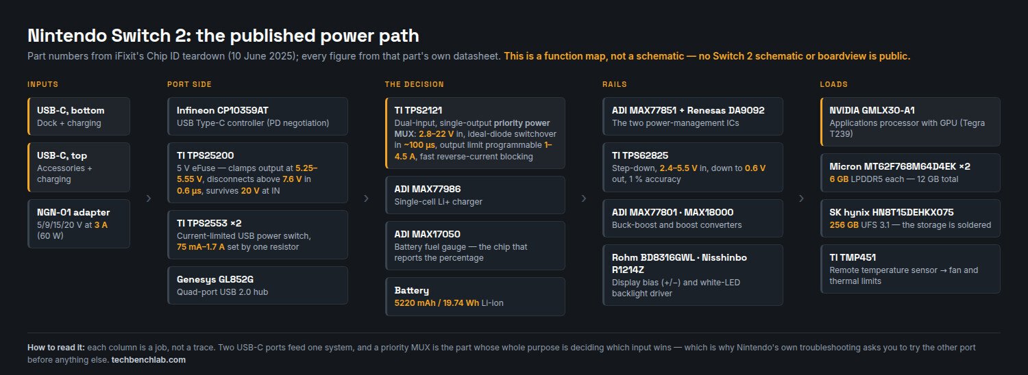
There is no Switch 2 schematic and no boardview in circulation. What exists is iFixit’s Chip ID teardown (10 June 2025, credited to Shahram Mokhtari with contributor Chunglin Chin), which photographs both sides of the board and labels the packages. Three callouts are prefixed “Likely” — the teardown’s own hedge, worth keeping — and one accelerometer/gyroscope is attributed to STMicroelectronics with no part number at all.
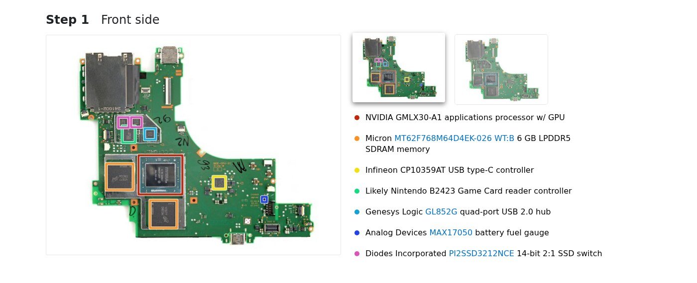
Grouped by job, with the numbers read from the manufacturer’s datasheet rather than from the teardown:
| Part | Job on this board | The number that matters at the bench |
|---|---|---|
| NVIDIA GMLX30-A1 | Applications processor with GPU (Tegra T239) | Nothing public — no datasheet, no reference design |
| Micron MT62F768M64D4EK-026 WT:B ×2 | LPDDR5 system memory | 6 GB per package — the 12 GB on the spec sheet is two parts, not one |
| SK hynix HN8T15DEHKX075 | 256 GB NAND with UFS 3.1 controller | Soldered. There is no storage swap on this console |
| Infineon CP10359AT | USB Type-C controller (PD negotiation) | No public datasheet for this part number |
| TI TPS2121 | Dual-input, single-output priority power MUX | 2.8–22 V inputs, 56 mΩ on-resistance, output limit set by resistor between 1 A and 4.5 A, ideal-diode switchover in 100 µs typical, fast reverse-current blocking |
| TI TPS25200 | 5 V eFuse | Clamps its output to 5.25–5.55 V, disconnects above 7.6 V in 0.6 µs, answers a short in 3.5 µs, tolerates 20 V at IN, 60 mΩ, up to 2.6 A |
| TI TPS2553 (three placements) | Current-limited power distribution switch | Limit programmed by one external resistor, anywhere from 75 mA to 1.7 A, ±6 % accuracy |
| TI TPS62825 | Step-down converter | 2.4–5.5 V in, regulates down to 0.6 V out at 1 % accuracy, 4 µA quiescent |
| ADI MAX77851SAWJ + Renesas DA9092 | The two power-management ICs | Neither has a public datasheet — these are exactly the parts a rail tree would need |
| ADI MAX77986 · MAX17050 | Single-cell Li+ charger · battery fuel gauge | The gauge reports the percentage, so a gauge fault reads to the user as a battery fault |
| ADI MAX77801 · “Likely” MAX18000 | Buck-boost and boost converters | The boost is flagged “Likely” — treat that part number as unconfirmed |
| Rohm BD8316GWL · Nisshinbo R1214Z | Display bias (positive and inverted) · white-LED backlight driver | Backlight-dead and image-dead split here, before the panel |
| Genesys Logic GL852G | Quad-port USB 2.0 hub | Four downstream ports behind one upstream link |
| TI TMP451 | Remote temperature sensor | Reads the processor’s own junction diode — fan behaviour and thermal limits follow this chip, not the heatsink |
| “Likely” Nintendo B2423 | Game card reader controller | Nintendo silicon, undocumented anywhere — card-slot faults have no published signal chain |
| MediaTek MT3681AEN · Realtek ALC5658 · Intelligo IG2200 | Wi-Fi 6 and Bluetooth · audio codec · voice processor | Mic path and headphone path are different chips: a dead jack is not a dead codec |
Inside a Joy-Con 2, the teardown names eight more: TI BQ25618 (1.5 A single-cell charger, 20 mA termination, JEITA profile over I²C, 1 A boost), MediaTek MT3689BCA Bluetooth SoC, ADI MAX98388 class-D amplifier, NXP PN7160B1HN NFC controller, TDK-InvenSense ICM-42607-PN six-axis IMU, AKM AK09919C three-axis compass, another TPS2553, and a “Likely” MAX3864xA.
2,985 fault reports, counted
Method, so you can repeat it or disagree with it. Every post from 1 June 2025 to 21 September 2026 in three subreddits where people open hardware — r/consolerepair (19,846 posts), r/NintendoSwitchHelp (16,886) and r/SwitchHacks (6,303) — pulled from the Arctic Shift public Reddit archive: 43,035 threads. Title and body matched against switch ?2|switch2|ns2|joy-?con ?2 give 8,553 threads, of which 2,985 also carry fault vocabulary (broken, won't, dead, repair, drift, cracked, damaged, RMA, warranty, error, no power, not charging, bricked…). The ranking labels titles only, which is stricter than labelling bodies: 1,528 of the 2,985 titles carry at least one label, and a title can carry two.
| What the title is about | Threads | Share of 2,985 fault reports |
|---|---|---|
| Joy-Con 2: drift, magnets, pairing, rail | 361 | 12.1 % |
| Screen: cracks, dead pixels, backlight, touch | 334 | 11.2 % |
| Dock, HDMI, TV output | 253 | 8.5 % |
| System software: update, error code, brick | 176 | 5.9 % |
| Charging and the USB-C ports | 123 | 4.1 % |
| Wi-Fi / Bluetooth | 99 | 3.3 % |
| Audio: speakers, jack, microphone | 91 | 3.0 % |
| Battery: life, 90 % charge limit, swelling | 84 | 2.8 % |
| Buttons, kickstand, hinge, shell | 77 | 2.6 % |
| Game card slot | 66 | 2.2 % |
| Fan, heat, thermal | 58 | 1.9 % |
| microSD Express | 55 | 1.8 % |
| No power, black screen, won’t wake | 44 | 1.5 % |
| Liquid damage | 15 | 0.5 % |
That is the shape of a healthy first year: the top two rows are a detachable controller and a glass panel, the two parts a user breaks without the board having any opinion about it. The electrically interesting failures are thin and specific. Eight threads describe smoke or burning at a charging port, from “Nintendo switch 2 top charging port smoking” (July 2025, 88 comments) to “Switch 2 charging plug burning itself?” a year later. Nine describe Nintendo attributing a failure to liquid damage and declining warranty service — the sharpest quotes €258 for a USB-C connector. Six report a microSD Express card that will not read, starting on launch day itself. The monthly curve: 535 fault reports in June 2025, 289 in July, then a floor of 119 to 200 a month for the following year — the spike is people learning a new machine, the floor is the real traffic.
The Switch 2 has barely entered the repair channel
Restrict the count to r/consolerepair — the one sub in this corpus where people open consoles for money — and the Switch 2 appears in 88 of 19,846 threads, 0.44 %. Over the identical window, the PlayStation 5 appears in 14.47 %, the PS4 in 9.08 %, the original Switch family in 5.78 %, Xbox Series X|S in 3.86 %. Seventy-two of those 88 report a fault, and they are parts jobs: joystick replacements, a game-card shell swap, a waterlogged unit, a charge port.
The strict board-level count across all 8,553 Switch 2 threads is two. One asks how to test the fan. The other, from 19 August 2025, is titled “Nintendo switch 2 Boardview.” — someone asking for the file that still does not exist. That is the honest state of this console at component level: named, photographed, and not yet reverse-engineered.
The part nobody covers: two USB-C ports and one priority MUX
The Switch 2 has two power-capable USB-C ports — bottom for the dock and charging, top for accessories and charging. The official adapter, model NGN-01, is a 60 W USB-PD supply: 5.0 V/3.0 A, 9.0 V/3.0 A, 15.0 V/3.0 A, 20.0 V/3.0 A. Nintendo’s charging article states the third-party floor plainly: “An AC adapter with an output of 54W or more can be used, but please note, unlicensed products do not undergo Nintendo’s testing and evaluation process.”
Two inputs, one system — and the board carries a part whose entire job is deciding between two inputs. The TPS2121 is a dual-input, single-output priority MUX: 2.8–22 V in, priority given either to the higher input or to one you nominate, crossover in about 100 µs without letting the output sag, and reverse-current blocking fast enough that the losing input never back-feeds. The 22 V ceiling is the interesting part: a 20 V PD contract fits inside it, a 5 V eFuse rail does not. Those are different parts on different rails, which is why the TPS25200’s 5.25–5.55 V clamp tells you nothing about what a bad 20 V charger does to the dock port.
It also explains why Nintendo’s troubleshooting asks you, before anything else, to try the other USB-C port. Read as a bench test rather than customer advice, that step separates two failure domains:
- Charges on one port, not the other. The fault sits upstream of the MUX, on that port’s own front end — connector, its power switch, or the Type-C controller. The second port is your evidence, not a workaround. Thirty-eight threads in the corpus are already doing this comparison by hand, usually without knowing why it works.
- Charges on neither, with an adapter that works on another device. You are past the ports and into shared territory: the MUX, the charger, the gauge, or a rail that never comes up. Nintendo’s own escalation agrees — no battery icon at all after 15 to 30 minutes on a known-good NGN-01 is where they stop troubleshooting and take the console in.
Two things make this less satisfying than it sounds. The MUX’s current limit is set by an external resistor, so the real ceiling on this board is a number nobody has published. And the two parts you would need to build a rail tree — MAX77851 and DA9092 — are precisely the two with no public datasheet. You can name the power path on this console; you cannot yet put expected voltages on it. That is the honest difference between this page and our MacBook Air M2 power sequence, where the rails are documented.
If one lands on your bench
Confirm the adapter first — NGN-01, or a PD supply of 54 W or more, proven on another device — then use the second port as an A/B test before opening anything. If you do open it, iFixit’s guides and parts cover the mechanical layer (battery, fan, screen, card reader, Joy-Con connectors, board removal), and that is where the realistic work is today. At component level the current-draw triage on a lab supply still applies: draws nothing, draws normal current with no image, or dead short are three different jobs, and none of them needs a schematic. What you cannot do yet is check a rail against a published value.
Limits of this data
Counting threads measures conversation, not failure rates. A console inside warranty goes back to Nintendo and never generates a repair post; a drifting Joy-Con generates several. r/NintendoSwitchHelp contributes 2,904 of the 2,985 fault reports, so the corpus leans owner, not technician, and software complaints are under-represented by the choice of subs. Keyword labelling over-counts common words such as dock and battery, and it is one language on one platform. Nothing here was measured on a console: every electrical figure comes from the datasheet of the part iFixit identified, and every identification is iFixit’s, including its three “Likely” hedges.
FAQ
Is there a Switch 2 schematic or boardview? No. In 15 months the corpus contains a single request for one and no release. The public identification is iFixit’s Chip ID teardown.
Can I charge it with any USB-C charger? Nintendo’s own answer is a wattage floor, not a brand: 54 W or more, with the caveat that unlicensed supplies are not tested by Nintendo. The official NGN-01 tops out at 20 V/3 A.
Why does it stop charging at about 90 %? Because of a setting, not a fault — Nintendo’s charging article names it: “Stop battery charging at approximately 90%”. It is the first thing to rule out before anyone opens a console for a charging complaint.
Sources
- iFixit, Nintendo Switch 2 Chip ID (teardown, 10 June 2025) and the Nintendo Switch 2 device page (specifications, guides, parts).
- Nintendo Support, Nintendo Switch 2 Cannot Be Charged and System Has No Power, a Blank Screen, or Won’t Wake Up.
- Nintendo, Nintendo Switch 2 AC Adapter main specifications.
- Texas Instruments datasheets: TPS2120/TPS2121 (SLVSEA3F), TPS25200 (SLVSCJ0F), TPS2552/TPS2553 (SLVS841F), TPS6282x (SLVSEF9I), TMP451, BQ25618/619 (SLUSDF8F).
- Micron, MT62F768M64D4EK-026 WT:B part detail.
- Reddit corpus via the Arctic Shift public archive API, pulled 21 September 2026: r/consolerepair, r/NintendoSwitchHelp, r/SwitchHacks, 1 June 2025 to 21 September 2026.
Related on this site
- MacBook Air M2 power sequence — what a board map looks like when the rails are documented.
- How to read a boardview — the tool this console has no file for yet.
- Bench power supply diagnostics — current draw first, component hunting second.
- The six BMS cutoffs — when a “dead battery” is a protection doing its job.
- US right-to-repair tracker — who has to publish what, and when.