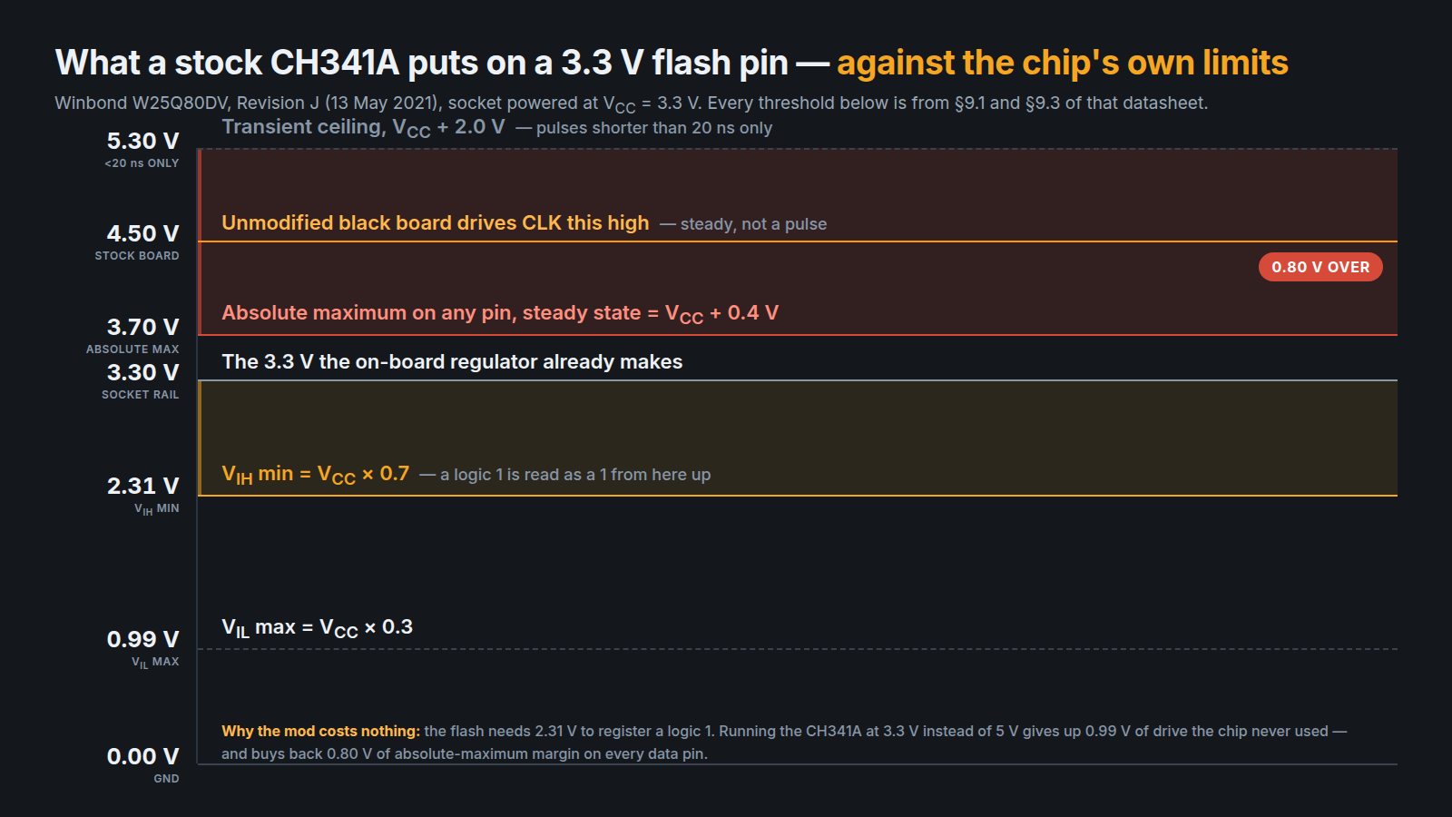
An unmodified black CH341A drives its data lines to about 4.5 V while the socket feeds the flash chip 3.3 V. Against the chip’s own datasheet that stops being vague: a Winbond W25Q80DV on a 3.3 V rail has an absolute maximum of 3.70 V on any pin — so the programmer sits 0.80 V over the limit, to deliver a logic 1 that only needed 2.31 V.
⬇ AsProgrammer 2.1.2 and the CH341 driver (Windows)
Download AsProgrammer 2.1.2
Download CH341 driver
No software fixes the problem below. It is hardware, and it is on the board before any chip goes in the socket. Install walkthrough: our CH341A and AsProgrammer guide.
What the 5 V actually violates
The fault is visible in the schematic. The board has an AMS1117-3.3 regulator, but it only powers the socket; the CH341A keeps its own VCC pin (pin 28) on the USB 5 V rail. As One Transistor’s teardown puts it, “the chip is powered from 5V, so its I/O ports will also use 5V.” Their scope capture of the clock reads 4.5 V; the EEVblog thread on the same board reports “over 4.7V” on CS, MOSI and CLK.
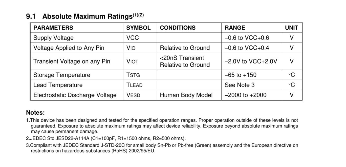
Here is what that means for the part most people are flashing. Every limit below is from the Winbond W25Q80DV datasheet, Revision J (13 May 2021), §9.1 and §9.3, socket rail at 3.3 V.
| Datasheet limit | Formula | At VCC = 3.3 V | Where 4.5 V lands |
| Input high voltage, VIH min | VCC × 0.7 | 2.31 V | 2.19 V more than the chip needs |
| Operating supply, VCC | — | 2.7 – 3.6 V | — |
| Voltage applied to any pin, VIO | −0.6 to VCC + 0.4 | 3.70 V | 0.80 V over, continuously |
| Transient voltage, VIOT | −2.0 to VCC + 2.0 | 5.30 V | Inside it — but only for pulses under 20 ns |
That last row is why the internet argues about this. A 4.5 V spike would be legal; a 4.5 V level is not. The datasheet says exposure beyond absolute maximum ratings “may cause permanent damage”, while exposure to them “may affect device reliability” — a reliability problem, not an instant kill, which is why one person reads fifty chips without incident and the next bricks a board.
Which board do you have? Don’t trust the version number
The silkscreen revision settles nothing — OpenIPC’s wiki blames versions “prior ver. 1.7”, while boards marked V1.7 are sold both with and without on-board level conversion. Judge by what you can see.
| What you have | Data lines | What to do |
| Matte black board, capacitor C4 on the opposite side of the crystal | ≈4.5–4.7 V | Mod it, or add a level shifter |
| Black board with gold trim edges, C4 beside the crystal (units shipping by 2025) | 3.3 V by default | Nothing — it was redesigned |
| Blue CH341A/B board | Set by two jumpers | Set them to 3.3 V before anything else |
| Board sold as “1.8 V level conversion” | 1.8 V at the socket | Use it for W-suffix parts only |
| Any board plus a separate 1.8 V adapter | 1.8 V | Mandatory for 1.8 V flash — 3.3 V will not do |
The 30-second check that settles it: plug the programmer into USB with the socket empty and measure from GND to the MISO and MOSI pins. Around 5 V means unfixed; around 3.3 V means there is nothing to do.
The fix, three ways
All three move the CH341A’s own supply to the 3.3 V the board already makes. Pin 9 (V3) has to come along, which is why every version touches capacitor C4.
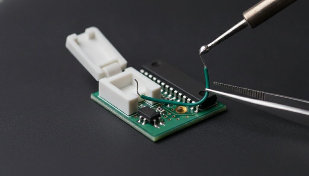
- Lift the pin. “No track cuts, just lift pin 28 … and run a wire from the lifted pin across to pin 9”, then tie that to the AMS1117’s centre (output) leg.
- Cut the trace. Sever the 5 V trace feeding pin 28 on the back of the board, then wire the regulator output to pin 28 and C4.
- Solderless. Scrape through the 5 V trace from the USB header and bridge the 3V3 and 5V pins at the far end of the header with a two-pin jumper. A knife and a jumper, no iron.
Flashing a GPU or motherboard BIOS
Read the chip marking first. Winbond puts the voltage in one letter: in W25Q80DVSNIG the V means 2.7–3.6 V, and a W there (W25Q80EW, W25Q128FW) means a 1.8 V part and a mandatory adapter. The trap is that the top-side marking is not the ordering number — the datasheet’s own table marks W25Q80DVSNIG as 25Q80DVNIG, dropping the W prefix and the package letter, so searching for what you read under the microscope returns nothing.
Then strip the target: Tom’s Hardware’s recovery guide says to “take everything off the board (all components and all connectors, even the 3v cell if it is detachable)”, so nothing back-feeds the rail you are about to drive. Red stripe to pin 1, the end with the dot. Read twice and compare before writing — if the dumps differ it is contact, not the chip, and our SOIC-8 clip guide works through that.
Problems people actually hit
“File size larger than IC size.” Auto-detect chose the wrong part; pick the chip manually from AsProgrammer’s list.
Reads fine, writes fail verification. Check that WP# and HOLD# are not held low by the target, and see the in-circuit caveats — on a populated board the flash shares its rail with everything else.
The ID reads but the dump is all FF. The clip has power and clock but not data. Reseat it; on an assembled board, remember the programmer is feeding the whole 3.3 V rail through eight tiny contacts.
Questions people ask
Mine has read dozens of chips unmodified — is this a myth? No. The EEVblog thread documenting the fault runs 24 posts from October 2017 to May 2020 and contains both outcomes: “I fried the PCB — its dead now” and “Nothing got short circuited, the world didn’t come to an end, and it just worked.” Reliability damage does not announce itself.
Doesn’t the 3.3 V jumper fix it? No. That jumper sets the socket rail; the CH341A’s own supply is untouched, which is why OpenIPC describes levels that “remain at 5V despite the programmer being set to 3.3V.”
Should I buy a different programmer instead? For 25-series SOIC-8 only, a fixed CH341A is fine. For NAND, eMMC or 48-pin parts see RT809H vs RT809F; for scripted work, flashrom drives the CH341A directly.
Sources
- Winbond W25Q80DV datasheet, Rev J — §9.1, §9.2, §9.3, §10.7 and §10.8.
- One Transistor — CH341A schematic and the 4.5 V clock capture.
- EEVblog — CH341A power supply fix, 24 posts, Oct 2017 – May 2020.
- flashrom — CH341A/B, including the blue board’s voltage jumpers.
- OpenIPC wiki — CH341A voltage fix (trace-cut version).
- Sawyer Shepherd — solderless fix (C4 telltale, gold-trim redesign).
- Chuck Nemeth — 3.3 V mod · Johannes’ blog — fix without lifting a pin.
- Tom’s Hardware — recovering a board from a bad BIOS flash.